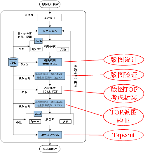
Chip layout design is a crucial aspect of the entire chip design process. The overall process can be categorized into front-end design (logic design) and back-end design (physical design). Front-end design focuses on realizing the logic circuit, encompassing requirement specification decomposition, detailed design, HDL coding, simulation verification, and logic synthesis. Back-end design, on the other hand, primarily involves chip layout design, converting the logic circuit into geometric figures that contain physical information such as device type, size, relative positioning, and interconnection. This results in a GDSII layout file, which is then provided to the wafer manufacturer for mask production and subsequent wafer manufacturing.
The chip layout is the culmination of the integrated circuit design process, significantly influencing the chip's functionality, performance, and manufacturing cost. Excellent chip performance hinges on meticulous layout design. Poorly designed layouts can lead to tape-out and product failures, causing substantial economic losses and delaying R&D progress for chip design companies.
The chip layout is the physical realization of the chip's logic circuit design and is closely tied to the chip's process node. Advances in downstream chip applications and rising performance demands have driven the number of transistors on integrated circuits to increase, pushing process nodes to evolve continuously. We have now reached advanced process nodes such as 16nm/14nm/10nm/7nm/5nm FinFET, with ongoing developments targeting 3nm-1nm. As process nodes evolve, integrated circuit device structures become more complex and layered, leading to a significant increase in layout design DRC workload and design complexity.
Compared to larger process nodes, advanced process nodes pose more stringent requirements on chip layout design, particularly in four key areas. Firstly, the self-heating effect is pronounced in advanced processes, elevating the risk of chip reliability issues. Secondly, the secondary effects of advanced processes are prominent, resulting in shrinking inspection windows in layout design, more detailed regulations, and increasing design complexity. Thirdly, the number of layout layers in advanced processes has increased, demanding high performance from computer image display, processing speed, simulation tools, accuracy, and design environments during the design process. Lastly, designers must not only possess extensive design experience but also have a thorough understanding of FinFET processes and advanced process development tools, necessitating heightened capabilities.
As such, the significance of chip layout design in the chip design and production process has become increasingly prominent. Providing high-performance, high-reliability, low-power, and low-cost layout designs through optimized design and routing is fundamental to chip design and development, especially for high-end chips, and holds immense importance.

Chip layout design includes the main processes

